GENERAL REQUIREMENTS
GENERAL REQUIREMENTS
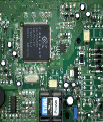
The printed wiring board (PWB) is an essential part of a total electronic circuit packaging system. The design requirements of the PWB must accommodate the various components required to achieve product functionality, while meeting packaging and other product design requirements.
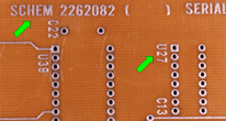
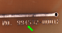
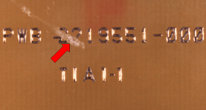
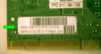
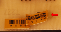
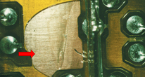
Boards shall be clean and damage-free, with sharply defined conductive patterns. Plating and solder mask shall be of uniform color and finish, holes properly located, markings sharply defined and aligned, and electrical/solder termination areas bright and shiny.
GENERAL REQUIREMENTS
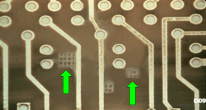
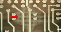
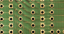
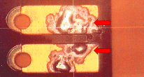
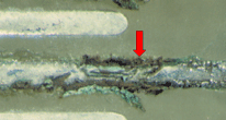
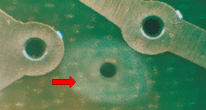
The printed wiring board is clean and damage-free, with sharply defined conductive patterns. Plated-Through Holes (PTH) and vias are properly located, clean and unfilled, and exhibit smooth and uniform plating. Electrical termination areas are bright and shiny. Solder mask exhibits proper registration.
Best Workmanship Practice
PREFERRED
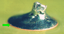
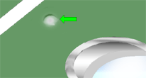
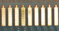
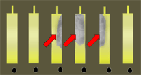
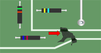
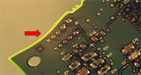
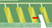
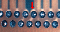
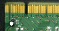
GOLD/PRECIOUS METAL CONTACTS
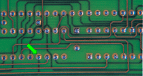
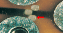
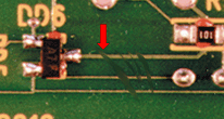
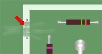
Contact surfaces are clean and bright, with a uniform and smooth finish.
Best Workmanship Practice


PREFERRED
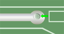
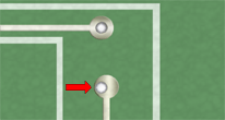
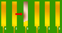
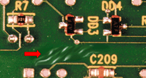
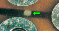
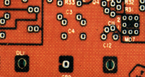
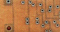
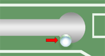
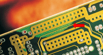
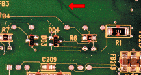
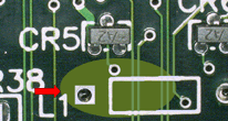
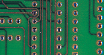
HOLE LOCATION/REGISTRATION
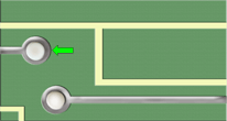
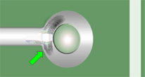
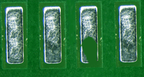
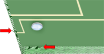
Holes (supported/unsupported) shall be centered in the lands and located per engineering documentation. Annular ring shall be concentric to the pad.
Best Workmanship Practice
PREFERRED
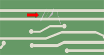
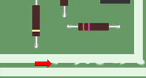
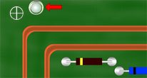
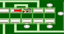
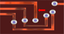
INTERFACIAL CONNECTIONS (VIAS)
DOUBLE-SIDED PWBs
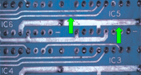
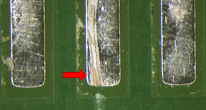
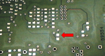
Vias in double-sided PWBs require the use of filler wire (Z-wire) for support if the PWB coupon has not been evaluated by construction analysis (micro-section).
NASA-STD-8739.3 [11.2.4.a]